Novel photonic devices, especially photonic integrated circuits (PICs) for transformative technologies, including high-speed optical communication and computing, ultrasensitive biochemical detection, efficient solar energy harvesting and super-resolution imaging. The design of these advanced devices is inevitably time consuming, which hindered their actual application in our daily life.
A team led by Prof. ZHANG WenFu from the Xi'an Institute of Optics and Precision Mechanics (XIOPM) of the Chinese Academy of Sciences (CAS) reported a novel genetic-algorithm-based deep neural network (GDNN) to efficiently design the photonic device. Their up-to-date result was published on Photonics Research.
Although the novel photonic devices are of great interests, which are normally designed by numerical simulations, the device satisfied certain operation requirements can be only depends on the designers’ experience.
Many numerical simulation algorithms such as finite element method (FEM) and finite difference time-domain (FDTD) method, which have been widely utilized in designing the specific photonic devices. However, these algorithms are still computation and time consuming. Therefore, a highly efficient design method is very important to accelerate the development of next-generation optical applications.
According to the researchers, the rapid development of deep neutral networks (DNNs) has greatly drawn their attention, and they successfully realize the highly efficient design of the PIC based on GDNN.
The GDNN-based inverse design in their work includes four parts: encoding, selection, forward and inverse design. The requirement simulation data of the proposed GDNN is less than 3000 to design several silicon photonics devices including power splitters with uncommon splitting ratios, a TE mode converter, and a broadband power splitter.
The results indicate that the algorithm exhibits great flexibility and ability in dealing with multiple design constrains. For example, the broadband power splitter is designed for as many as 11 optimization targets, and the optimal design exhibits a maximum insertion loss of 0.47 dB and good flatness over 400 nm wavelength range with a 2.5 μm × 1.5 μm footprint.
The presented GDNN algorithm can be widely implemented in designing many complex micro- and nanophotonic structures that could not be easily realized before.
This work was supported by the Strategic Priority Research Program of the Chinese Academy of Sciences, National Natural Science Foundation of China, Youth Innovation Promotion Association of Chinese Academy of Sciences, West Light Foundation of the Chinese Academy of Sciences, Natural Science Basic Research Program of Shaanxi and Research Project of Xi’an Postdoctoral Innovation Base.
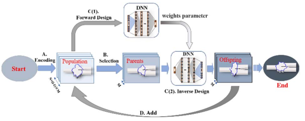
(Schematic diagram of the proposed DNN. (Image by XIOPM)