High power diode lasers based on GaAs material system have found a variety of applications such as solid-state laser and fiber laser pumping because of their excellent performance in power level, power conversion efficiency (PCE), and reliability. Therefore, increasing the output power of the diode laser bar is a high priority.
Many investigations have been proposed to efficiently improve the output power of the diode laser bar by intentionally optimizing the low-temperature operation. So far, the highest output power is 1.98 kW (2 kA) at a low heatsink temperature THS = 203 K in QCW operation, with the PCE of 64% at 1 kW. Although the value of output power is tempting, the low operation temperature inevitably restricted its practical applications. Are there any methods to realize high output power diode laser bar with room temperature operation?
A research team led by Prof. Dr. WANG ZhenFu from Xi'an Institute of Optics and Precision Mechanics (XIOPM) of the Chinese Academy of Sciences (CAS) proposed a 940-nm diode laser bar based on epitaxially stacked active regions by employing a tunnel junction structure and peak power of 1.91 kW was achieved at 25 °C. The results were published in IEEE PHOTONICS JOURNAL.
The epitaxially stacked double-junction structure. (Image by XIOPM)
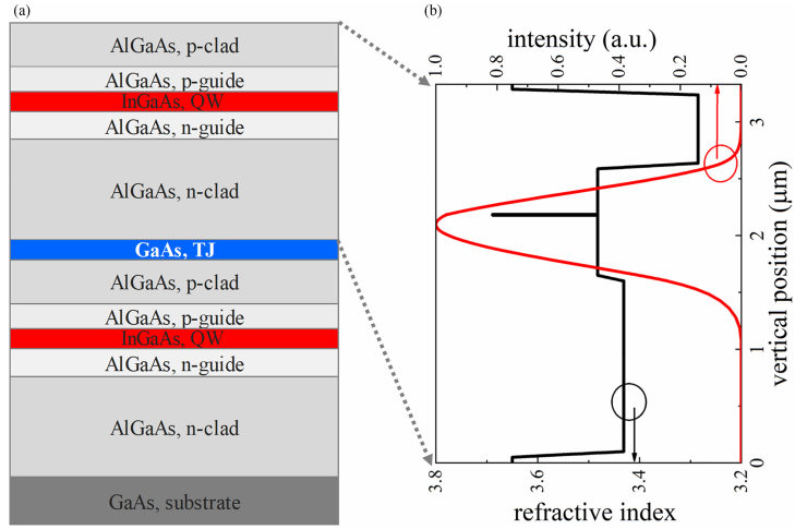
According to the researchers, the epitaxially stacked double-junction structure consists of two almost identical p-i-n structures connected by a GaAs tunnel junction (TJ). The difference between the two p-i-n structures is adjusted by the position of the GaAs TJ. The tunnel junction is 14-nm thick for both n-type and p-type layers and is doped to the levels of >3 × 1019 cm-3 with Te in the n-side and >1 × 1020 cm-3 in the p-side.
The epitaxial structure with double laser junctions was grown on n+ GaAs substrate by metal organic chemical vapor deposition (MOCVD). Then the wafers were processed using standard photolithography and wet-chemical etching, followed by SiNx deposition, metallization of Ti/Pt/Au as the p-electrode, substrate thinning, and deposition of AuGeNi/Au as the n-electrode.
The results indicate that the proposed high-power laser bar, based on the high-efficiency p-i-n structure and a low resistance single tunnel junction, achieve a record peak power of 1.91 kW was obtained at 1 kA drive current and 25 °C operation temperature.
The proposed method can provide another possible direction for further power improvement and brightness scaling from a single bar under room temperature operation.