Fundamental issues within conventional c-plane emitter materials, including efficiency droop, green gap, and blue shift, are limiting the development of solid-state lighting in both cost and performance. To address these issues, researchers and experts have been pursuing aggressively in semipolar and nonpolar materials.
Although semipolar and nonpolar GaN have great potentials, the implementation of orientations is still bottlenecked. The heteroepitaxy of semipolar and nonpolar GaN on sapphire suffers from a high density of stacking faults (SFs). How to successfully grow device-quality, large-area semipolar GaN on sapphire?
A research team led by Dr. WANG Jie from Xi'an Institute of Optics and Precision Mechanics (XIOPM) of the Chinese Academy of Sciences (CAS) presents a unique growth technology to eliminate the stacking faults (SFs) in semipolar GaN grown on sapphire. The result was published in PHYSICA STATUS SOLIDI B. (https://doi.org/10.1002/pssb.201900565.)
To completely eliminate the SFs, they have developed a unique growth technology called “facet controlled OCE” designated as Gen IV. The SFs may disappear if the N-polar GaN is eliminated during the heteroepitaxy. Based on the theory of kinetic Wulff plot, they developed a growth process to accelerate the growth rate of N-polar facet and then suppress the formation of the N-polar GaN during the heteroepitaxy.
Then, they exhibit the growth of semipolar GaN with any orientation on patterned substrate and achieve SF-free semipolar GaN heteroepitaxially grown on sapphire.
Based on this breakthrough, the dream of producing device-quality, large-area semipolar GaN in arbitrary surface orientations is becoming more realistic.
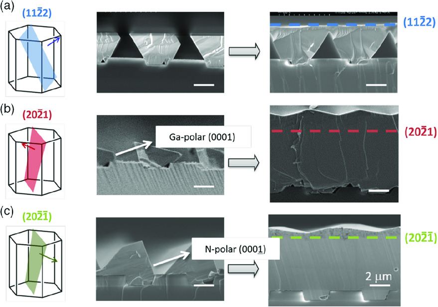 Cross‐sectional SEM images of GaN films grown on sapphire substrates. (Image by XIOPM)