The capacitance–voltage characteristics of metal–insulator–semiconductor structures based on Hg1xCdxTe (x = 0.218) with CdTe passivation are studied before and after the passivation annealing process. We found that after vacuum annealing at 300 °C for 24 h, the micromorphology of the passivation layer was significantly improved, and as the fixed charge density decreased from 1.3 × 1012 cm2 to 1.0 × 1010 cm2, the fast surface state density decreased from 2 × 1013 cm2 eV1 to 3 × 1012 cm2 eV1, with a minimum value of 1.2 × 1011 cm2 eV1. From these findings, combined with the secondary ion mass spectroscopy analysis, we conclude that the annealing process propagates an equivalent electrical surface for CdTe/HgCdTe uniformly from the principal physical interface to the inside of the bulk material, effectively improving the characteristics of the CdTe passivation layer.
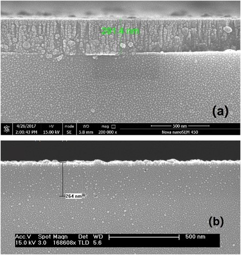
SEM image of the CdTe/HgCdTe interface