Atomic layer deposition (ALD) is utilized by a research team led by Prof. Dr. GUO Haitao from Xi'an Institute of Optics and Precision Mechanics (XIOPM) of the Chinese Academy of Sciences (CAS) to prepare thin MgO coatings 1–50 nm on Si substrate.
In addition, secondary electron emission (SEE) coefficient of MgO/Si double-layered structure is evaluated as a function of coating thickness and primary electron (PE) energy.
After neutralizing the surface of test specimen, they have accurately analyzed the relationship between secondary electron yield (SEY) of MgO coating and PE energy.
Meanwhile, SEE characteristics of MgO/Si double-layered structure have been systematically analyzed.
A maximum SEY value of 6.15 has been achieved at coating thickness of 30 nm and PE energy of 550 eV. Furthermore, theoretical model is established by using Dionne's SEE model to analyze experimentally measured SEY data, demonstrating consistency between experimentally measured and theoretically calculated results.
This work demonstrates that SEE level of MgO coating can be optimized by tuning coating thickness and presents novel insights into SEE characteristics of composite materials.
Those results can serve as a baseline for further design and fabrication of a wide array of electronic devices.
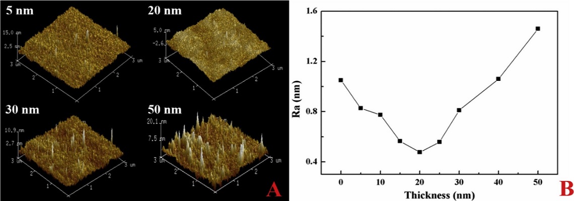
The scan size (3 μm × 3 μm) of 5 nm, 10 nm, 30 nm and 40 nm ALD-processed MgO coating. (Image by XIOPM)
(Original research article “Ceramics International” (2020) http://dx.doi.org/10.1016/j.ceramint.2019.12.067 )